


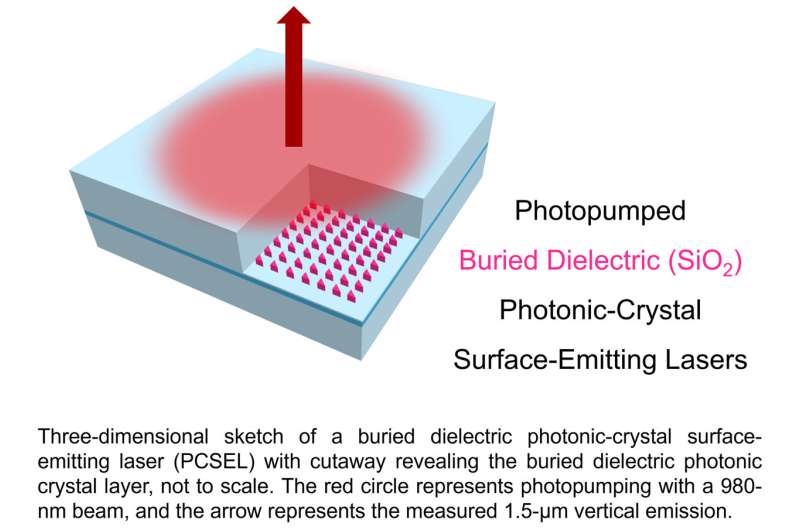
Researchers at the University of Illinois Urbana-Champaign have made a significant breakthrough by successfully demonstrating photopumped lasing from a buried dielectric photonic-crystal surface-emitting laser, which operates at room temperature. This innovative technology emits at an eye-safe wavelength, marking a first in the field and potentially enhancing various defense applications. The findings were published in the IEEE Photonics Journal.
For decades, the lab led by Kent Choquette, a professor of electrical and computer engineering, has focused on vertical-cavity surface-emitting lasers (VCSELs). These lasers are widely used in devices such as smartphones, laser printers, and barcode scanners. In early 2020, the Choquette lab shifted its focus to a new type of laser inspired by research from a Japanese group, known as photonic-crystal surface-emitting lasers (PCSELs). This new class of semiconductor lasers utilizes a photonic crystal layer to produce beams with desirable characteristics, including high brightness and precise spot sizes.
The research received funding from the Air Force Research Laboratory, allowing Choquette’s team to explore and advance the technology behind PCSELs. Graduate student Erin Raftery, the lead author of the paper, expressed optimism about the future of PCSELs, stating, “We believe PCSELs will be extremely important in the future. They just haven’t reached industrial maturity yet, and we wanted to contribute to that.”
PCSELs typically incorporate air holes within their design, which can become compromised when the semiconductor material is regrown around these features. To address this challenge, the researchers at Illinois replaced the air holes with a solid dielectric material. By embedding silicon dioxide within the semiconductor regrowth, they successfully demonstrated the first proof of concept for a PCSEL with buried dielectric features.
“The first time we tried to regrow the dielectric, we didn’t know if it was even possible,” Raftery noted. “Ideally, for semiconductor growth, you want to maintain that very pure crystal structure all the way up from the base layer, which is difficult to achieve with an amorphous material like silicon dioxide. But we were actually able to grow laterally around the dielectric material and coalesce on top.”
Looking ahead, experts in the field anticipate that these advanced lasers could play crucial roles in applications such as autonomous vehicles, laser cutting, welding, and free space communication over the next two decades. The research team plans to enhance their current design by integrating electrical contacts, enabling the laser to connect to a power source.
Choquette emphasized the collaborative effort behind this achievement, stating, “The combined expertise of Erin and members of the Minjoo Larry Lee group, as well as the facilities and expertise at the Air Force Research Laboratory on Wright-Patterson Air Force Base, were necessary to accomplish this result. We look forward to diode PCSEL operation.”
The implications of this research extend beyond theoretical interest, promising practical applications that could reshape industries reliant on laser technology. As the field continues to evolve, the advancements made by the Illinois Grainger engineers represent a significant step toward the industrial application of PCSELs.
For further details, refer to the publication: E. M. Raftery et al., “Photopumped Buried Dielectric Photonic-Crystal Surface-Emitting Lasers,” IEEE Photonics Journal (2025). DOI: 10.1109/JPHOT.2025.3561087.