


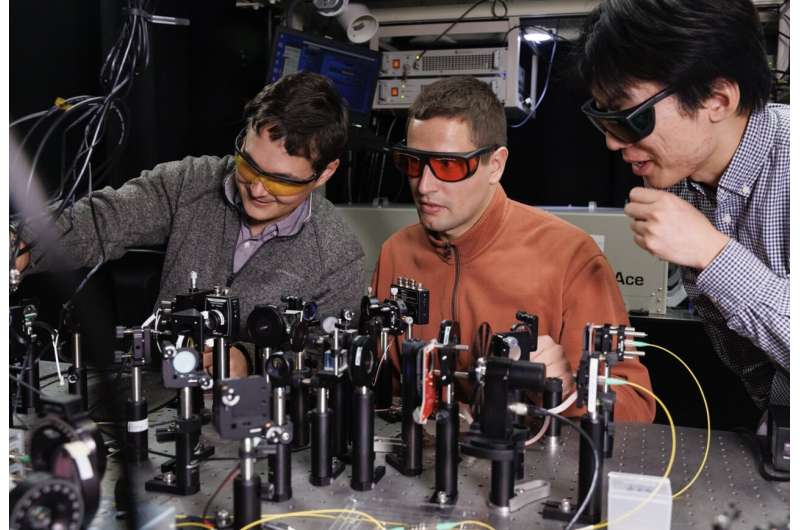
Researchers at Purdue University have made a significant advancement in the field of optical technology, achieving all-optical modulation in silicon by utilizing an electron avalanche process. This breakthrough, detailed in a paper published in Nature Nanotechnology on December 11, 2025, promises to enhance the performance of photonic and quantum systems critical for imaging, communication, and information processing.
Over the years, the development of photonic systems has been hampered by the limited optical nonlinearity of most materials used. Conventional materials fail to exhibit strong changes in response to varying light intensities, which is essential for creating ultrafast optical switches. These switches are vital components in fiber optics communication systems as well as in various photonic devices.
Understanding the Electron Avalanche Process
The research team, led by Demid V. Sychev and Vladimir M. Shalaev, sought to explore new strategies for controlling light solely with light. In their investigation, they recognized that existing ultrafast detection methods were limited and ineffective at the single-photon level. Sychev explained, “This led us to consider whether it might be possible to build an ultrafast modulator capable of switching a macroscopic optical beam in response to just a single photon.”
By leveraging the electron avalanche effect, the researchers developed a mechanism that enables all-optical modulation. This phenomenon involves a chain reaction where a single energized electron liberates additional electrons from atoms, generating a cascade of energized electrons. Sychev noted, “When a single photon generates one free electron, the strong electric field accelerates it, allowing it to gain even more energy.”
Innovative Modulation Strategy
In their experiments, the researchers illuminated silicon with light at a single-photon intensity, triggering the electron avalanche. This process resulted in a substantial increase in the material’s electrical conductivity and reflectivity, similar to the behavior of a photodiode. “Importantly, the greater the number of free electrons generated, the stronger the ‘metallicity,'” Sychev stated, underscoring the scalability of their approach.
The team’s findings revealed that their modulation strategy significantly increased the nonlinear refractive index of the silicon device, outperforming other known materials. “The principle we outlined is unique in its ability to produce strong interactions between two optical beams, independent of their power or wavelength,” Sychev elaborated.
One of the key advantages of this approach is its reliance on the intrinsic properties of semiconductors, which could mitigate limitations tied to external components. As Sychev pointed out, “In future implementations, our principle could enable sub-THz and THz clock rates.” This innovative method operates effectively at room temperature and is compatible with existing complementary metal-oxide-semiconductor (CMOS) fabrication techniques.
The implications of this research extend beyond basic optical modulation. The electron avalanche-based strategy could pave the way for the development of ultrafast optical switches, essential for scaling up photonic circuits and advancing quantum technologies. Sychev expressed optimism about the future applications, stating, “Such technologies could find use across a variety of information-processing tasks, including computing and communication.”
While the current findings do not preserve coherence between interacting beams, they suggest potential for realizing all-optical quantum circuits capable of operating at exceptionally high clock rates. “With appropriate protocols, it may even assist in the implementation of certain photonic quantum gates,” Sychev added, indicating the transformative potential of their work.
The research team plans to further explore the intricacies of the avalanche process and its applications in practical devices. With continued theoretical and experimental studies, they aim to refine their approach to develop a single-photon switch suitable for real-world deployment. “We envision that this concept could open an entirely new research direction, ultimately enabling fully optical photonic circuits for both quantum and classical applications,” Sychev concluded.