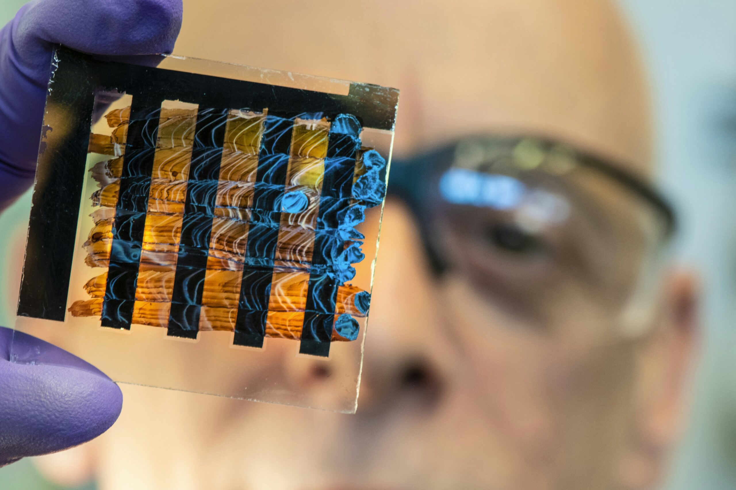
A collaborative effort among engineers from several prestigious institutions has led to the development of a revolutionary new 3D chip that has the potential to address significant limitations in artificial intelligence (AI) performance. Researchers from Stanford University, Carnegie Mellon University, the University of Pennsylvania, and the Massachusetts Institute of Technology partnered with SkyWater Technology, the largest U.S.-based pure-play semiconductor foundry, to create this innovative multilayer computer chip.
The newly designed chip differs from traditional flat, two-dimensional (2D) chips by employing a vertical architecture. This prototype features ultra-thin layers stacked like floors in a high-rise building, allowing for an unprecedented number of vertical connections. The unique design promotes faster data transfer, significantly enhancing the chip’s efficiency. Early testing indicates that this 3D chip outperforms its 2D counterparts by approximately four times, with projections suggesting even greater gains as more layers are added.
Addressing Limitations of Conventional Chips
The existing 2D chips face a critical challenge known as the “memory wall,” which occurs when processing speeds surpass the chip’s ability to deliver data efficiently. Large AI models, such as ChatGPT and Claude, require continuous access to vast amounts of data, yet conventional chips struggle to provide this due to their limited memory configurations and crowded pathways. Engineers have attempted to mitigate this issue by miniaturizing transistors, but they are approaching physical limits, often referred to as the “miniaturization wall.”
By constructing chips vertically, the team aims to overcome both challenges. As Tathagata Srimani, assistant professor of electrical and computer engineering at Carnegie Mellon University, explained, “By integrating memory and computation vertically, we can move a lot more information much quicker.” This approach not only enhances speed but also optimizes space, likening it to the efficient transportation found in high-rise buildings.
Innovative Manufacturing Techniques
Historically, many attempts to create 3D chips involved stacking separate chips, which often resulted in bottlenecks due to inadequate connections between layers. However, this research team adopted a monolithic 3D integration method, building each layer directly atop the previous one. This continuous flow allows for tighter packing and a greater number of connections, significantly improving performance.
As Mark Nelson, vice president of technology development operations at SkyWater Technology, highlighted, “Turning a cutting-edge academic concept into something a commercial fab can build is an enormous challenge.” This achievement illustrates that advanced architectures can be produced domestically and at scale, which is essential for maintaining U.S. leadership in semiconductor innovation.
The implications of this research extend beyond immediate performance gains. The architecture has the potential to deliver improvements in energy efficiency, targeting a reduction of up to 1,000-fold in energy delay product (EDP). By minimizing the distance data must travel and increasing the number of vertical pathways, the chip can enhance throughput while lowering energy consumption.
The research team is already looking ahead. They anticipate that further refinement of the chip design will yield even greater advancements for real AI workloads, including applications derived from Meta’s open-source LLaMA model. The prospect of enhanced performance provides a compelling vision for the future of AI hardware, with the possibility of reshaping how technology addresses complex computational tasks.
Research and development efforts took place at several institutions, including the Stanford University School of Engineering and the Carnegie Mellon University College of Engineering, and all chip fabrication occurred at SkyWater Technology’s facility in Bloomington, Minnesota. The project received support from various organizations, including the Defense Advanced Research Projects Agency and the U.S. National Science Foundation.
As the researchers emphasize, the progress made with this 3D chip not only signifies performance enhancement but also represents a shift toward a new era of domestic semiconductor innovation. The need for engineers trained in these advanced methods is critical, mirroring the educational push that fueled the integrated circuit boom in the 1980s. Through initiatives like the Microelectronics Commons California-Pacific-Northwest AI Hardware Hub, a new generation of engineers is being prepared to drive the future of American semiconductor innovation.
In conclusion, breakthroughs such as this 3D chip are pivotal for the continued advancement of AI technology. As the team, led by principal investigator Subhasish Mitra from Stanford University, noted, “If we can build advanced 3D chips, we can innovate faster, respond faster, and shape the future of AI hardware.”


